Electron microscopes help reveal mysteries in our microscopic world and have already found application in a variety of fields, from semiconductor devices to medical. To make observations at increasingly quantum orders of magnitude, Hitachi started working on the development of the ultimate electron microscope in 2010. Then, following a development period of about five years after the inception of the project, Hitachi succeeded in creating the world's first*1 43-pm (picometer)*2 resolution microscope.
Video: The World's Highest Resolution Electron Microscope

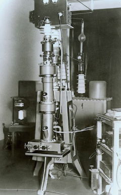
HU-2 electron microscope developed as the first commercial model in Japan in 1942
Electron microscopes have become an essential tool for industrial development, utilized in a wide range of fields such as semiconductor devices and materials, as well as in biology and healthcare. The first transmission electron microscope was invented in Germany in 1932, while in Japan, research & development into applications began in 1939. Hitachi produced the first commercial model in Japan, the HU-2, and supplied it to Nagoya Imperial University in 1942. Hitachi has been leading the world in the development of electron microscopes since that time.
In the 1970s, Dr. Akira Tonomura, a researcher with Hitachi, came up the idea to use holography to make observation of smaller objects possible. To many people, the term "holography" will bring to mind the anti-counterfeiting holograms incorporated into banknotes. However, the technology was first invented as a way of improving the resolution of electron microscopes. Hitachi started working on developing higher performance electron microscopes and advancing research in electron beam holography. Hitachi succeeded in the development of the first practical holography electron microscope in 1978.
The holography electron microscope utilizes the properties of electrons as waves to observe and measure microscopic activity. By making it possible to observe subtle electrical and magnetic fields directly, this technology helps researchers see into the unpredictable world of quantum physics where objects behave in ways that often defy common sense.

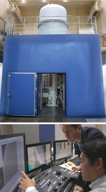
Atomic Resolution Holography Electron Microscope (above) and control board (below)
In 2000, Hitachi and the University of Tokyo jointly developed the world's first 1-MV ultra-high-voltage holography electron microscope with support from the Japanese government. This contributed to elucidating the mechanism of high temperature oxide superconductors by providing a direct view of magnetic flux in the superconductors. After the development of the 1-MV holography electron microscope, Dr. Tonomura came up with an idea for the ultimate holography electron microscope. This was in response to the new development of viable correctors for spherical aberrations present in electron microscope lenses, a technology with the potential to dramatically improve the resolution of holography electron microscope. Performance targets were set for resolution in the 40-pm range (the best resolution possible at the time was in the 70-pm range) with the ability to measure electromagnetic fields in three dimensions, etc.
However, it was not easy to incorporate a corrector for spherical aberration into the lens of an ultra-high-voltage electron microscope unit. To get the best performance from the spherical aberration corrector required improvements in the stability of the electron microscope unit by a factor of more than two. No group in the world had previously grappled with such a difficult problem using electron microscopes that were so large in size. So Hitachi began research and development of the necessary technologies to be able to successfully incorporate a spherical aberration corrector into an ultra-high-voltage electron microscope.
In 2010, Hitachi's work on the ultimate electron microscope was selected for the "Funding Program for World-Leading Innovative R&D on Science and Technology" (FIRST Program), becoming a national project for Japan. Development of the ultimate electron microscope began in full force. However, the project went through a number of unexpected setbacks in its development process. Portions of the project suffered serious damage from the Great East Japan Earthquake and Tsunami in 2011. Two key team members, Isao Matsui, a leading engineer on the project, and Dr. Tonomura, who had been the leading researcher organizing work on the entire project, passed away during the project. Even so, project members who succeeded them persevered and overcame various difficulties. They completed the development of a 1.2-MV holography electron microscope and achieved the target resolution (40-pm range) in November 2014.
The new electron microscope was developed by solving numerous technical obstacles to dramatically improve its resolution. Focal blur occurs regardless of the presence of a spherical aberration corrector if the energy dispersion of the electron beam is high. To prevent this, Hitachi developed a number of components, including resistors and a specialized high-voltage power supply cable to reduce instability in the energy of the 1.2 MeV electron beam. The electron gun was developed to produce a stable electron beam that could be used for a long period of time without recalibration. Hitachi also constructed a special reinforced building designed to house the electron microscope in a controlled and stable environment. It included walls lined with acoustic absorbent material and systems to minimize changes in temperature. The building was designed to provide a high degree of sound insulation and low acoustic noise and to reduce floor vibration. To minimize magnetic fields, the area around the electron microscope was enclosed in permalloy to provide magnetic shielding. By solving these technical issues and dramatically improving the stability of the device, Hitachi was able to successfully implement a spherical aberration corrector in a high-voltage electron microscope for the first time in the world.
In an experiment performed using monocrystalline tungsten, the Hitachi researchers succeeded in imaging its structure at a resolution of 43 pm (the world's highest resolution). The researchers were also able to observe the position of atoms in a sample of gallium nitride (GaN) with a separation of 44 pm, confirming that the new electron microscope can be used to observe and measure the structure and electromagnetic fields of a specimen at an atomic resolution.
Published paper: (T. Akashi et al, Appl. Phys. Lett. 106, 074101 (2015))

Hitachi succeeded in demonstrating performance of the 1.2-MV atomic resolution holography electron microscope, imaging the 44-pm spacing between gallium (Ga) atoms in crystalline GaN.
Beyond having the world's highest resolution, the real potential in Hitachi's new atomic resolution holography electron microscope comes from its ability to observe and measure electromagnetic fields at an atomic resolution. The specific nature of a material is influenced by the internal electromagnetic fields in the material. The key to success in developing innovative functional materials with new capabilities or superior performance is being able to observe and measure those electromagnetic properties at an atomic resolution.
High-performance magnets, large-capacity secondary batteries, materials for ultra-low energy consumption memory devices and high-temperature superconducting materials are all being born from the understanding of quantum phenomena in electromagnetic fields at the atomic level. In cooperation with RIKEN* and other world-leading research organizations, Hitachi continues to work on research and development that will contribute to the creation of new materials to advance social innovation.
Release Date: March 2016
Solutions By: Research & Development Group, Hitachi, Ltd.


